Workshop A5, Xin Bao Industrial Zone, building C, Shenzhen szjklsm_pcb@163.com / mkt@szjkyl-pcb.com 0755-27338957 / 18682274874
English
精科裕隆-高端PCB制造商
Current Position:Home > 制造能力> PCB process capability
PCB Process Capability
Project Project name Process Capability
Overall process capability Layers 1-30 layers
High Frequency Hybrid HDI Ceramic materials and PTFE materials can only be mechanically drilled for blind buried holes, controlled depth drilling, back drilling, etc. (laser drilling is not allowed, and copper foil cannot be directly pressed)
High-speed HDI Made as regular HDI
Laser order Levels 1-5 (≥6 levels require review)
Plate thickness range 0.1-5.0mm (less than 0.2mm, more than 6.5mm to be reviewed)
Minimum finished product size Veneer 5*5mm (less than 3mm to be reviewed)
Maximum finished product size 2-20 floors 21*33inch; Note: if the short edge of the board edge exceeds 21inch, it needs to be reviewed.
Maximum finished copper thickness Outer layer 8oz (larger than 8oz to be reviewed), inner layer 6oz (larger than 6oz to be reviewed)
Minimum finished copper thickness 1/2oz
Interlayer alignment ≤3mil
Through hole filling range Plate thickness ≤ 0.6mm, hole diameter ≤ 0.2mm
Thickness range of resin plug orifice plate 0.254-6.0mm, PTFE plate resin plug hole needs to be reviewed.
Plate thickness tolerance Plate thickness ≤ 1.0mm; ±0.1mm
Plate thickness > 1.0mm; ±10%
Impedance tolerance ±5Ω(<50Ω),±10%(≥50Ω); ± 8% (≥ 50 Ω, to be reviewed)
Warpage Routine: 0.75%, limit: 0.5% (to be reviewed) maximum: 2.0%
Pressing times Pressing of the same core plate ≤ 5 times (more than 3 times need to be reviewed)
Material type Ordinary TG FR4 Shengyi S1141, Jiantao kb6160a, Guoji gf212
Medium TG FR4 Shengyi s1150g (medium TG plate), Jiantao kb6165f, Jiantao kb6165g (halogen free)
High Tg FR4 Shengyi s1165 (halogen-free), Jiantao kb6167g (halogen-free), Jiantao kb6167f
Aluminum substrate Guoji gl12, clear cs-al-88/89 ad2, Juqin jq-143 1-8 mixed pressure FR-4
Type of material used for HDI board Ldpp (it-180a 1037 and 1086), general 106 and 1080
High CTI Shengyi s1600
High Tg FR4 Isola:FR408、FR408HR、IS410、FR406、GETEK、PCL-370HR;联茂:IT-180A、
IT-150DA; Nelco:N4000-13、N4000-13EP、N4000-13SI、N4000-13EP
SI;松下:R-5775K(Megtron6)、R-5725(Megtron4);建滔:KB6167F;
台光:EM-827; 宏仁:GA-170;南亚:NP-180;台耀:TU-752、TU-662;
日立:MCL-BE-67G(H)、MCL-E-679(W)、 MCL-E-679F(J);腾辉:VT-47;
Ceramic powder filled high frequency materials Rogers:Rogers4350、Rogers4003;Arlon:25FR、25N;
Polytetrafluoroethylene high frequency material Rogers series、Taconic series、Arlon series、Nelco series、TP series
PTFE semi cured sheet Taconic:TP series、TPN series、HT1.5(1.5mil)、Fastrise series
Mixed pressure of materials Rogers、Taconic、Arlon、Nelco and FR-4
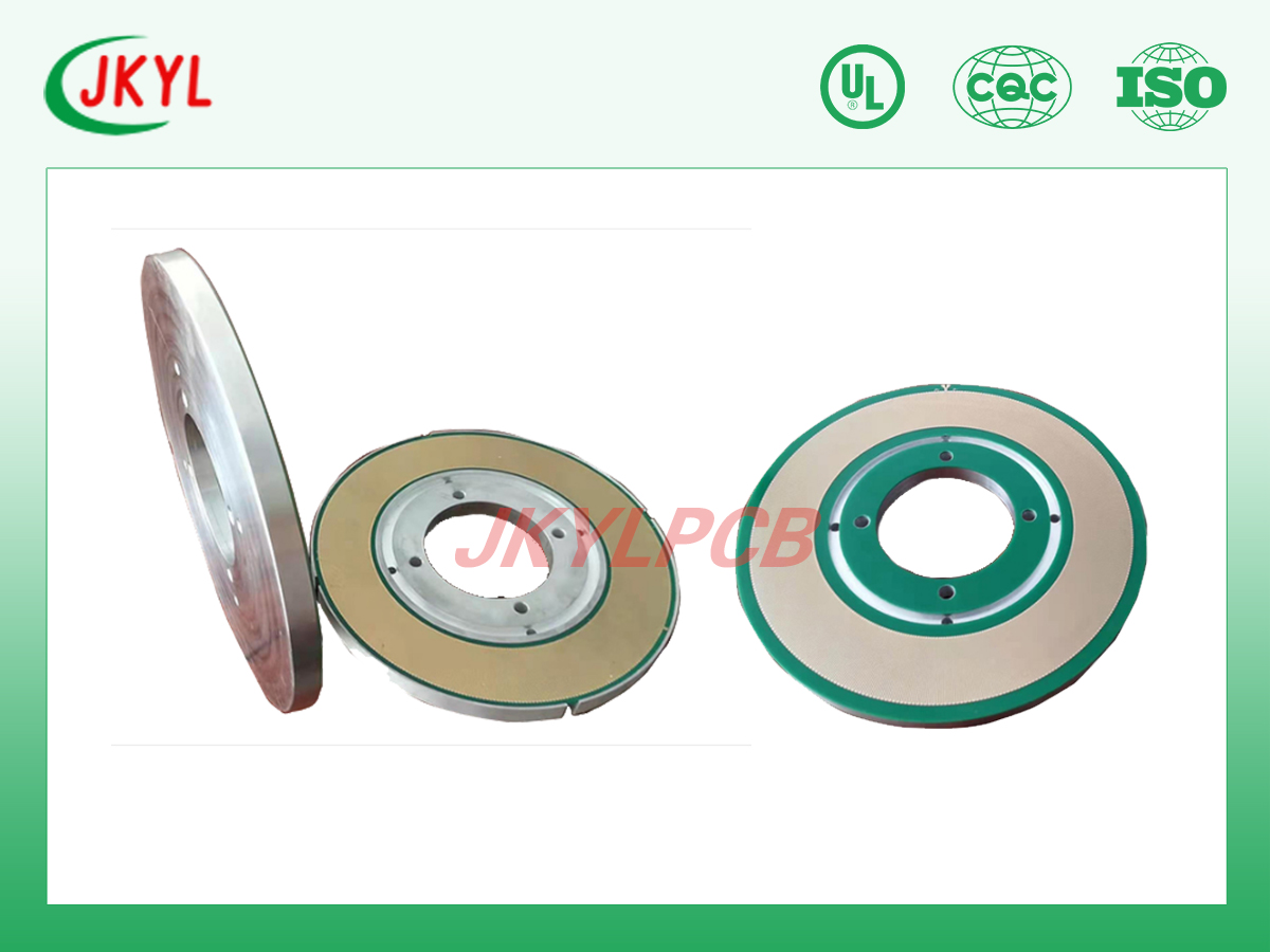
Metal substrate Number of layers Aluminum substrate and copper substrate: 1-8 layers; Cold plate, sintered plate, embedded metal plate: 2-24 layers; Ceramic plate: 1-2 layers;
Finished product size (aluminum substrate, copper substrate, cold plate, sintered plate, embedded metal plate) MAX:610*610mm、MIN:5*5mm
Maximum production size (ceramic plate) 100*100mm
Finished plate thickness 0.5-5.0mm
Copper thickness 0.5-10 OZ
Metal base thickness 0.5-4.5mm
Metal based material AL:1100/1050/2124/5052/6061;Copper:Red copper pure iron
Minimum finished hole diameter and tolerance NPTH:0.5±0.05mm;PTH(Aluminum substrate, copper substrate):0.3±0.1mm;PTH(Cold plate, sintered plate, embedded metal plate):0.2±0.10mm;
Profile machining accuracy ±0.2mm
Surface treatment process of PCB part Lead / non lead tin spraying; OSP; Nickel (palladium) gold precipitation; Electric (nickel) soft / hard gold; Electroplated tin; Nickel free electroplating of soft and hard gold; Thick gold production
Metal surface treatment Copper: nickel plated gold; Aluminum: anodic oxidation, hard oxidation, chemical passivation; Mechanical treatment: dry sand blasting and wire drawing.
Metal based materials Quanbao aluminum substrate (T-110, t-111); Tenghui aluminum substrate (vt-4a1, vt-4a2, vt-4a3); Laird aluminum substrate (1ka04, 1ka06); Bages metal substrate (mp06503, ht04503); Taconic metal substrate (tly-5, tly-5f);
Thickness of thermal conductive adhesive (dielectric layer) 75-150um
Size of buried copper block 3*3mm—70*80mm
Flatness of buried copper block (drop accuracy) ±40um
Distance from buried copper block to hole wall ≥12mil
Thermal conductivity 0.3-3W/m.k(Aluminum substrate, copper substrate, cold plate);8.33W/m.k(Sintered plate);0.35-30W/m.k(Buried metal plate);24-180W/m.k(Ceramic plate);
Product type Rigid plate Backplane, HDI, multilayer buried blind hole, thick copper plate, thick copper for power supply, semiconductor test board
Stacking mode Multiple pressing blind buried orifice plate Pressing on the same side ≤ 3
HDI board type 1+n+1, 1+1+n+1+1, 2+n+2, 3+n+3 (embedded hole in n ≤ 0.3mm), laser blind hole can be electroplated and filled
Local mixed pressure Minimum distance from mechanical drilling to conductor in local mixed pressure area ≤ 10 layers: 14mil; 12 floors: 15mil; > 12th floor: 18mil
Minimum distance from local mixed pressure junction to borehole ≤ 12 layers: 12mil; > 12th floor: 15mil
Surface treatment Unleaded Electroplating copper nickel gold, gold precipitation, hard gold plating (with / without nickel), gold finger, lead-free tin spraying, OSP, chemical nickel palladium, soft gold plating (with / without nickel), silver precipitation, tin precipitation, enig+osp, enig+g/f, full plate gold plating +g/f, silver precipitation +g/f, tin precipitation +g/f
Lead Lead spray tin
Thickness diameter ratio 10: 1 (lead / lead-free tin spraying, chemical precipitation of nickel gold, silver, tin, chemical nickel palladium); 8:1(OSP)
Machining dimension (max) Gold deposition: 520*800mm, vertical tin deposition: 500*600mm, horizontal tin deposition: less than 500mm on one side; Horizontal silver deposition: less than 500mm on one side; Lead / lead-free tin spraying: 520*650mm; OSP: single side less than 500mm; Electroplated hard gold: 450*500mm; One side is not allowed to exceed 520mm
Machining dimension (min) Tin deposition: 60*80mm; Silver deposit: 60*80mm; Lead / lead-free tin spraying: 150*230mm; OSP:60*80mm; At the surface of the walking board less than the above size
Thickness of processed plate Gold sinking: 0.2-7.0mm, tin sinking: 0.3-7.0mm (vertical tin sinking line), 0.3-3.0mm (horizontal line); Silver deposit: 0.3-3.0mm; Lead / lead-free tin spraying: 0.6-3.5mm; Tin spray plates below 0.4mm need to be reviewed and manufactured; OSP:0.3-3.0mm; Electroplated hard gold: 0.3-5.0mm (plate thickness ratio 10:1)
Minimum spacing between IC of gold plate or pad to line 3mil
Maximum height of golden finger 1.5inch
Minimum spacing between golden fingers 6mil
Minimum segment spacing of segmented golden finger 7.5mil
Surface coating thickness Tin spraying 2-40um (the thinnest thickness of the large tin surface with lead spraying is 0.4um, and the thinnest thickness of the large tin surface without lead spraying is 1.5um)
OSP Film thickness: 0.2-0.4um
Chemical precipitation of nickel and gold Nickel thickness: 3-5um; Gold thickness: 1-3uinch, ≥ 3uinch needs to be reviewed
Chemical precipitation of silver 6-12uinch
Chemical precipitation of tin Tin thickness ≥ 1um
Electroplate hard gold 2-50uinch
Electroplated soft gold Gold thickness 0.10-1.5um (dry film plating process), gold thickness 0.10-4.0um (non dry film plating process)
Chemical nickel palladium NI:3-5um,Pd:1-6uinch,Au:1-4uinch
Electroplating copper nickel gold The thickness of gold is 0.025-0.10um, the thickness of nickel is ≥ 3um, and the thickness of base copper is 1oz at most
Gold finger nickel plated gold Gold thickness 1-50uinch (the required value refers to the thinnest point), Nickel thickness ≥ 3um
Carbon oil 10-50μm
Green oil Copper cover oil (10-18um), through hole cover oil (5-8um), line corner ≥ 5um (primary printing, copper thickness less than 48um)
Blue gum 0.20-0.80mm
Drill hole Maximum plate thickness of 0.1/0.15/0.2mm mechanical drilling 0.8mm/1.5mm/2.5mm
Minimum laser drilling hole diameter 0.1mm
Maximum laser drilling aperture 0.15mm
Mechanical hole diameter (finished product) 0.10-6.2mm (corresponding to drilling tool 0.15-6.3mm)
The minimum finished hole diameter of PTFE material (including mixed pressure) plate is 0.25mm (corresponding to drill tool 0.35mm)
Hole diameter of mechanical buried blind hole ≤ 0.3mm (corresponding to drilling tool 0.4mm)
Hole diameter of green oil plug hole in disc hole ≤ 0.45mm (corresponding to drill tool 0.55mm)
The minimum hole diameter of connecting hole is 0.35mm (corresponding to 0.45mm of drilling tool)
The minimum diameter of metallized half hole is 0.30mm (corresponding to 0.4mm of drilling tool)
Maximum thickness diameter ratio of through-hole plate 20: 1 (excluding tool diameter ≤ 0.2mm; > 12:1 to be evaluated)
Maximum ratio of laser drilling depth to aperture 1:1
Mechanical depth control drill has the largest blind hole depth to hole diameter ratio 1.3:1 (aperture ≤ 0.20mm), 1.15:1 (aperture ≥ 0.25mm)
Minimum depth of mechanical depth control drill (back drill) 0.2mm
Drilling - minimum distance from mechanical drilling to conductor (non buried blind hole plate and first-order laser blind hole) 5.5mil (≤ 8 layers); 6.5mil(10-14); 7mil (> 14 floors)
Drilling - minimum distance from mechanical drilling to conductor (mechanical buried blind hole plate and second-order laser buried blind hole) 7mil (primary pressing); 8mil (secondary pressing); 9MIL (three times of pressing)
Drilling - minimum distance from mechanical drilling to conductor (laser blind hole) 7mil(1+N+1); 8mil (1+1+n+1+1 or 2+n+2)
Drilling - minimum distance from laser drilling to conductor (1st and 2nd order HDI board) 5mil
Drilling - minimum distance between hole walls of different networks (after compensation) 10mil
Drilling - minimum distance between the hole walls of the same network (after compensation) 6mil(通孔;激光盲孔);10mil(机械盲埋孔)
Drilling - minimum distance between non-metallic hole walls (after compensation) 8mil
Drilling hole position tolerance (compared with CAD data) ±2mil
Drilling - minimum tolerance of npth hole diameter ±2mil
Drilling - hole diameter accuracy of solderless devices ±2mil
Drilling - taper hole depth tolerance ±0.15mm
Drilling - taper hole orifice diameter tolerance ±0.15mm
Pad (ring) Minimum size of inner and outer pads of laser hole 10mil (4mil laser hole), 11mil (5MIL laser hole)
The size of inner and outer pads of mechanical via is the smallest 16mil (8mil aperture)
BGA pad diameter minimum There are lead tin spraying process 10mil, lead-free tin spraying process 12mil, and other processes 7mil
Pad tolerance (BGA) +/-1.2mil (pad < 12mil)+/- 10% (pad ≥ 12mil)
Line width / spacing Limit line width corresponding to copper thickness
1/2OZ:3/3mil
1OZ: 3/4mil
2OZ: 5/5mil
3OZ: 7/7mil
4OZ: 12/12mil
5OZ: 16/16mil
6OZ: 20/20mil
7OZ: 24/24mil
8OZ: 28/28mil
9OZ: 30/30mil
10OZ: 32/30mil
Line width tolerance ≤10mil:+/-1.0mil
>10mil:+/-1.5mil
Solder resist character Maximum drilling diameter of resistance welding plug hole (cover oil on both sides) 0.5mm
Solder resist ink color Green, yellow, black, blue, red, white, purple, matte green, matte oil black, high refraction white oil
Character ink color White, yellow, black
Maximum diameter of blue glue aluminum plug hole 5mm
Resin plug hole drilling hole diameter range 0.1-1.0mm
Maximum thickness diameter ratio of resin plug hole 12:1
Minimum width of resistance welding Bridge Special requirements for green oil 4mil and variegated 6mil controlled solder bridge
Minimum character line width White characters 3mil high 24mil; Black character 5MIL high 32mil
Minimum spacing of hollow words Hollow width 8mil height 40mil
Solder mask hollow word Hollow width 8mil height 40mil
appearance Distance from the center line of V-CUT without copper leakage to the figure H ≤ 1.0mm:0.3mm (20 ° refers to the angle of V-shaped incision), 0.33mm (30 °), 0.37mm (45 °);
1.0<H≤1.6mm:0.36mm(20°)、0.4mm(30°)、0.5mm(45°);
1.6<H≤2.4mm:0.42mm(20°)、0.51mm(30°)、0.64mm(45°);
2.4<H≤3.2mm:0.47mm(20°)、0.59mm(30°)、0.77mm(45°);
V-CUT symmetry tolerance ±4mil
The number of V-CUT lines is the largest 100
V-CUT angle tolerance ± 5 degrees
V-CUT angle specification 20、30、45 degrees
Chamfer angle of golden finger 20、30、45 degrees
Chamfer angle tolerance of gold finger ±5degrees
The minimum distance between tab and golden finger without falling injury 6mm
Minimum distance between the side of golden finger and the contour edge line 8mil
Depth accuracy (npth) of deep milling groove (edge) ±0.10mm
Overall dimension accuracy (edge to edge) ±8mil
Minimum tolerance of milling groove hole (PTH) Groove width and groove length are ± 0.15mm
Minimum tolerance of milling groove and hole (npth) Groove width and groove length are ± 0.10mm
Minimum tolerance for slotted holes (PTH) Groove width direction ± 0.075mm; Slot length / slot width < 2: Groove length direction +/-0.1mm; Slot length / slot width ≥ 2: slot length direction +/-0.075mm
Minimum tolerance for slotted holes (npth) Groove width direction ± 0.05mm; Slot length / slot width < 2: Slot length direction +/-0.075mm; Slot length / slot width ≥ 2: slot length direction +/-0.05mm


0755-27338957