Printed circuit boards are the most important part of modern electronic equipment. What exactly is a PCB? How to make microscopic and complex circuits on a PCB?
In the early days, electronic components were manually connected point-to-point with wires, a manual construction that was prone to error and difficult to scale up; and because these circuits were so complex, it was extremely difficult to repair damaged circuits.
In 1936, Paul Eisler (PAUL EISLER) recognized the drawbacks of traditional circuits and invented printed conductive copper circuits, which are traces on non-conductive boards to connect components.
And now the PCB has become much more complex!
The current PCB production starts with a common copper clad laminate and then drills some pilot holes.
After the engineer designs the circuit correctly, use the pcb design software to generate files such as gerber and drilling. According to these design files, the drilling machine drills holes. It should be noted that after drilling, the board should be properly cleaned to avoid leaving holes. the remains.
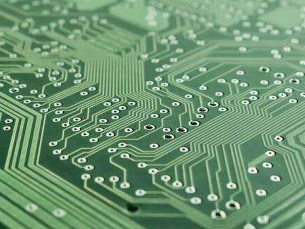
The next most important step is to create a complex conductive pattern, which requires an etching process. The part of the dry film that has not been irradiated by ultraviolet rays is dissolved in an alkaline solution of 60 to 120 degrees Celsius, and the part that has been irradiated by ultraviolet rays and has undergone polymerization is retained,
After this, drill holes on the PCB according to the dimensions and coordinates of the vias in the file. Then there is the copper sinking, that is, a layer of chemical thin copper is deposited on the originally non-conductive substrate (hole wall) and the copper surface. Next is the printing of green oil and characters, and the final step is comprehensive inspection.