1. The definition of processing level is not clear.
Design a single panel on the TOP layer. If you do not explain the positive and negative, it may not be easy to solder the resulting board when it is installed on the equipment.
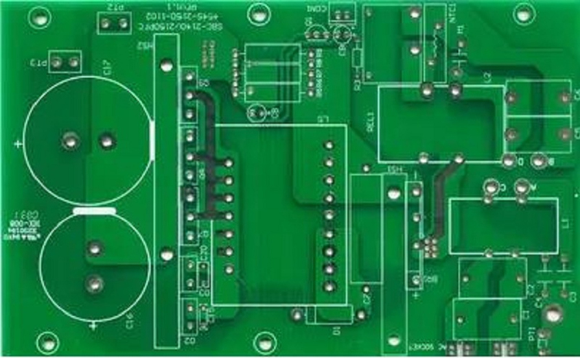
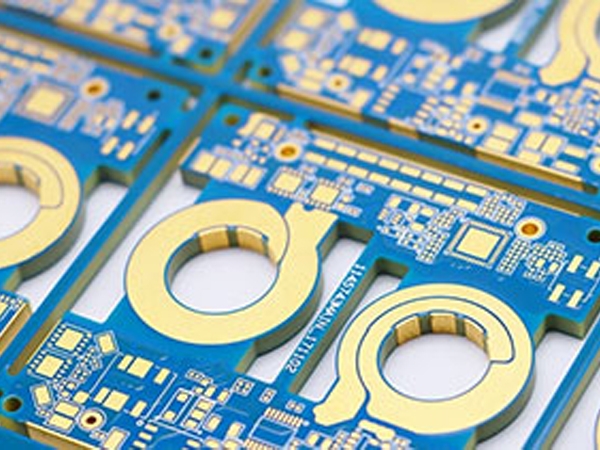
2. The large area of copper foil is too close to the outer frame.
The distance between the large area copper foil and the outer frame should be at least 0.2 mm, because when milling the shape, if the copper foil is milled, it is easy to cause the copper foil to warp and the solder resist to fall off.
3. Draw pads with fill blocks.
Using the pad to draw the pad can be checked by DRC when designing the circuit, but it is not suitable for processing, so this type of pad cannot directly generate solder mask data. When the solder mask is applied, the pad area will be covered by the solder mask. Difficulty in soldering the device.
4. The electrical ground is also a flower pad and a connection.
Due to the design of flower pad power supply, the ground plane is the opposite of the image on the actual printed board and all connections are isolated wires. Be careful when drawing several groups of power supplies or several ground isolation lines, so as not to leave gaps to short-circuit the two sets of power supplies, and the connection area cannot be blocked.