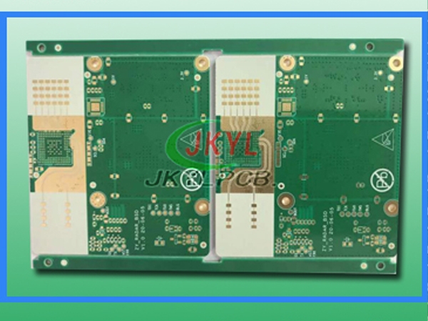
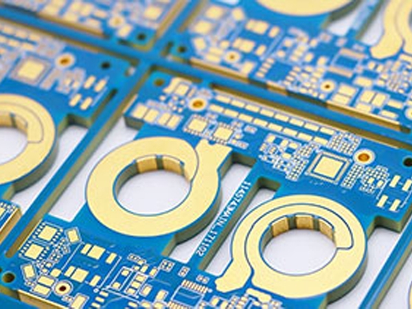
The pcb board printing process mainly passes through equipment, pads, vias, traces, silk screen, and solder mask positioning holes.
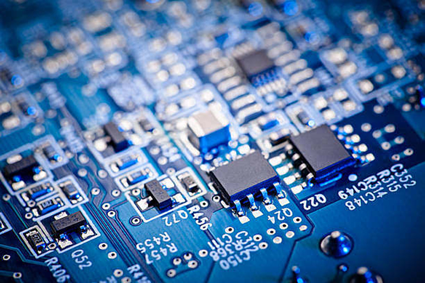
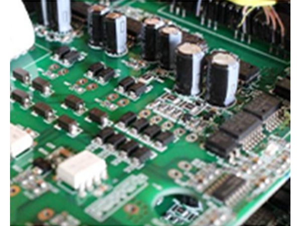
pcb board: components soldered on the pcb board, which is also the role of the pcb, presented on the pcb board in the form of pads + silk screen.
Soldering the board: Electrically connect the pins of the component equipment to the board, which corresponds to the pins of the equipment.
Trace: The signal wire that connects the pins of the device depends on the nature of the signal, the magnitude of the current, the speed, etc., the length and width of the trace, and so on.
Vias: Assuming that the pcb board circuit cannot complete all signal traces on one layer, the signal lines must be connected across layers through the via method. The method and aperture of the vias depend on the signal characteristics and processing requirements.