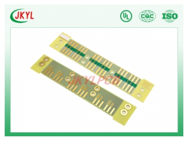
What are the classification and composition of vias on car camera circuit boards?
Vias are an important part of automotive camera circuit boards, and the cost of drilling usually accounts for 30% to 40% of the cost of automotive camera circuit boards. Simply put, every hole on the car camera circuit board can be called a via. So, what are the classification and composition of the vias of the car camera circuit board?
1, the classification of vias
In terms of function, vias can be divided into two categories: one is used for electrical connection between layers; the other is used for fixing or positioning components. In terms of process, vias are divided into three categories, namely blind vias, buried vias and through vias.
Blind holes are located on the top and bottom surfaces of the circuit board, with a certain depth, and are used for the connection of surface layers and inner layers. The depth of the holes usually does not exceed a certain ratio (diameter).
Buried vias are connection holes located in the inner layer of the circuit board and do not extend to the surface of the circuit board. The above two types of holes are located in the inner layer of the circuit board, and are completed by the through hole forming process before lamination.
Through holes refer to the holes that pass through the entire circuit board and can be used for internal interconnection or as mounting positioning holes for components. Because the through hole is easier to realize in the process and the cost is lower, it is used in most of the automotive camera circuit board proofing.
2. The composition of vias
From the design point of view, the via is mainly composed of two parts, one is the drill hole in the middle, and the other is the pad area around the drill hole. The size of these two parts determines the size of the via. When designing high-speed, high-density automotive camera circuit boards, designers always want the vias to be as small as possible, so that more wiring space can be left on the board. However, the reduction in hole size brings an increase in cost, and the size of the via hole is limited by process technologies such as drilling and electroplating: the smaller the hole, the longer it takes to drill, and the easier it is to deviate from the center position; and When the depth of the hole exceeds 6 times the diameter of the drilled hole, there is no guarantee that the hole wall can be uniformly plated with copper.