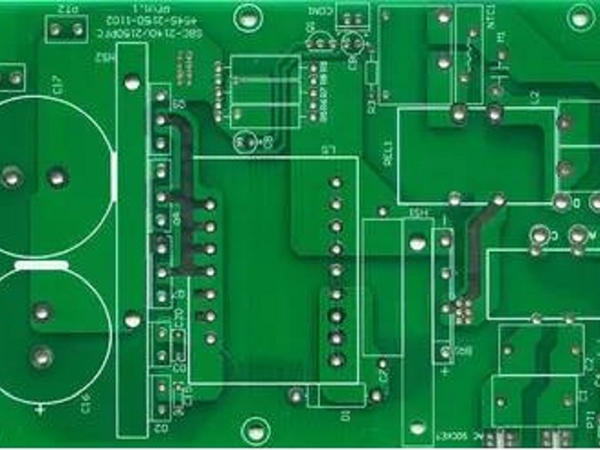
Multi-layer PCB circuit board companies often encounter the problem of "the hole is too close to the line, which exceeds the process capability". When we design the PCB board, the most consideration is how the wiring can connect each layer to the network signal line in the most reasonable way. on the connection. The denser the high-speed PCB board lines, the greater the density of vias (VIAs) placed, and the vias can play the role of electrical connection between layers.
So, what difficulties will the near hole cause to production? What near hole problems should we pay attention to? The following will tell you one by one.
1. If the two holes are too close during the drilling operation, it will affect the aging of the PCB drilling process. After drilling the first hole, the material in one direction will be too thin when drilling the second hole, resulting in uneven force on the drill tip and uneven heat dissipation of the drill tip, resulting in broken drill tip, resulting in PCB hole collapse. Beautiful or leak drilling does not conduct.
2. The vias in the multi-layer PCB will have hole rings on each layer of the circuit, and the surrounding environment of each hole ring is different, with or without clipping. When the CAM engineer of the PCB board factory optimizes the file, he will cut off a part of the hole ring when the clip wire is too close or the hole is too close to the hole, so as to ensure that there is a safe distance of 3mil between the solder ring and the different network copper/wire .
3. The hole position tolerance of drilling is ≤0.05mm. When the tolerance goes to the upper limit, the multilayer board will have the following situations:
(1) When the lines are dense, there are small gaps between vias and other elements 360° irregularly. To ensure a safe spacing of 3mil, the pads may be cut in multiple directions.
(2) Calculated according to the source file data, the hole edge to the line edge is 6 mil, the hole ring is 4 mil, and the ring to the line is only 2 mil. To ensure a safe distance of 3 mil between the ring and the line, the 1 mil welding ring needs to be cut, and the pad after cutting is only 3 mil. . When the hole position tolerance offset is the upper limit of 0.05mm (2mil), the hole ring is only 1mil left.
4. There will be a small amount of offset in the same direction in PCB production, the direction of the pads being cut is irregular, and the worst phenomenon will cause individual holes to break the solder ring.
5. The influence of lamination deviation in PCB multilayer board. Taking a six-layer board as an example, two core boards + copper foil are pressed together to form a six-layer board. During the pressing process, there may be a deviation of ≤0.05mm when the core board 1 and the core board 2 are pressed together, and the inner layer hole will also have a 360° irregular deviation after the pressing.
From the above problems, it can be concluded that the PCB board yield and PCB board production efficiency are affected by the drilling process. If the hole ring is too small and there is no complete copper protection around the hole, although the PCB can pass the open and short test and there will be no problems in the use of the previous product, the long-term reliability is still not enough.
Therefore, suggestions for multi-layer PCB board, high-speed PCB board hole-to-hole, hole-to-line spacing are given:
(1) Multilayer board inner layer hole to wire to copper:
Layer 4: Don't care
6 layers: ≥6mil
8 layers: ≥7mil
10 layers or more: ≥8mil
(2) Through hole inner diameter edge spacing:
Same network via: ≥8mil(0.2mm)
Different network vias: ≥12mil (0.3mm)